Fast - Precise - Scalable
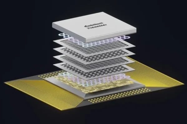
TAILORED MICRO- AND NANO-SCALE FABRICATION SERVICES
From process definition to device realization, leveraging multi-site cleanroom capabilities.


WHAT CAN WE DO?
Our Capabilities
Through partnerships with leading research institutes, we have access to state-of-the-art fabrication and characterization tools. This enables clients to prototype, fabricate, and test devices without in-house infrastructure


What do we serve?
OUR R&D SERVICES
At Micro to Nano Solutions, our low-volume fabrication service enables high-precision builds without the overhead of mass production. Whether you’re validating a new device concept or preparing early-stage samples, we deliver limited-run batches with process discipline, consistent quality, and the flexibility needed for advanced R&D cycles.
Our workflow ensures every design receives focused engineering attention—from materials selection to device finishing—so you can iterate efficiently and accelerate innovation at any scale.
Develop, test, and refine new ideas rapidly. Our prototype fabrication service supports fast turnarounds for concept validation and early device development.
What we offer:
- Quick-turn wafer and die-level fabrication
- Custom test structures for electrical, optical, or reliability studies
- Support for UV, e-beam, and direct-write lithography
- Flexible sample quantities with no strict minimums
Ideal for engineers refining device physics, microLED concepts, MEMS structures, or new material integrations.
Expertise in scalability, cost analysis, and process integration for pre-production readiness.
Guidance from early concept to pre-production readiness. We offer engineering expertise that bridges R&D and scalable manufacturing.
Consulting focus areas include:
- Scalability assessment of process flows and device structures
- Cost modeling, BOM analysis, and process trade-off evaluation
- Integration pathways toward pilot lines or foundry transfer
- Risk identification and mitigation strategies for transition to volume
Electrical, optical, and structural testing to ensure stability, reproducibility, and performance.
Ensure confidence in performance with rigorous analytical testing. We provide electrical, optical, and structural characterization to help you understand device behavior and material properties at every stage.
Characterization offerings include:
- I–V, C–V, and reliability electrical measurements
- Optical analysis for microLED, photonic, or thin-film devices
- Structural and surface evaluation (profilometry, microscopy, thin-film metrology)
- Failure analysis and parametric drift monitoring
Expertise in scalability, cost analysis, and process integration for pre-production readiness.
Guidance from early concept to pre-production readiness. We offer engineering expertise that bridges R&D and scalable manufacturing.
Consulting focus areas include:
- Scalability assessment of process flows and device structures
- Cost modeling, BOM analysis, and process trade-off evaluation
- Integration pathways toward pilot lines or foundry transfer
- Risk identification and mitigation strategies for transition to volume

Our engineers are available to discuss your requirements and explore how our capabilities can support your work.
WHAT YOU NEED TO KNOW ABOUT THE COVID-19
Frequently Asked Questions
-
What is novel coronavirus?
A novel coronavirus is a new coronavirus that has not been previously identified. The virus causing coronavirus disease 2019 (COVID-19), is not the same as the coronaviruses that commonly circulate among humans and cause mild illness, like the common cold. Patients with coronavirus COVID-19 will be evaluated and cared for differently than patients with common coronavirus diagnosis. -
How does virus spreads?
The virus that causes COVID-19 is thought to spread mainly from person to person, mainly through respiratory droplets produced when an infected person coughs or sneezes. These droplets can land in the mouths or noses of people who are nearby or possibly be inhaled into the lungs. Spread is more likely when people are in close contact with one another (within about 6 feet). -
What is the source of virus?
COVID-19 is caused by a coronavirus called SARS-CoV-2. Coronaviruses are a large family of viruses that are common in people and may different species of animals, including camels, cattle, cats, and bats. Rarely, animal coronaviruses can infect people and then spread between people. This occurred with MERS-CoV and SARS-CoV, and now with the virus that causes COVID-19. -
How can people help stop COVID-19?
People can fight stigma by providing social support in situations where you notice this is occurring. Stigma affects the emotional or mental health of stigmatized groups and the communities they live in. Stopping stigma is important to making communities and community members resilient. See resources on mental health and coping during COVID-19.
How can we help?
Tell us about your project, and our team will get back to you in 24 hours
Trusted collaborations with leading companies and research institutions
Academic & Research Facilities